
The introduction of 3D printing has revolutionized manufacturing and electronic product design in the past few years. From making pharmaceutical drugs on demand to creating cost-efficient and less dense parts for the automotive industry, it’s now being used for a whole lot of applications, and printed circuit boards are no exception.
While currently in its infancy, 3D-printed circuit boards have the potential to shorten prototyping cycles and increase precision in PCB production.
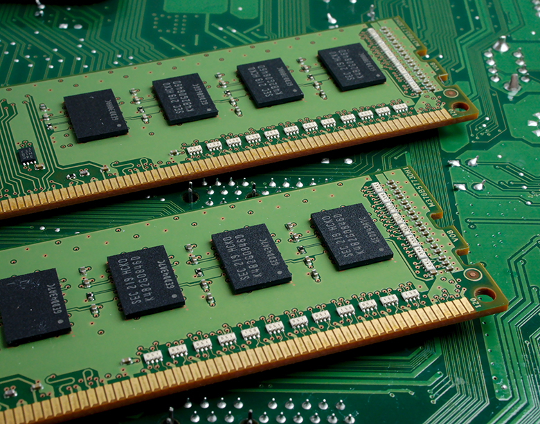
To refresh, printed circuit boards enable manufacturers to create complex wiring circuitry and organize them in a relatively compact surface within electronic product designs.
It’s also the backbone of many devices we have today — including your phone and even the smallest of IoT (Internet of Things) sensors. Nonetheless, for engineers and hobbyists, it’s still costly and time-consuming to make, which is why 3D printing circuit boards have a broad appeal.
Are you curious about who works on our PCBs at MAKO Design + Invent? Check out our #MeetMako Blog on our electrical designer, Navdeep!
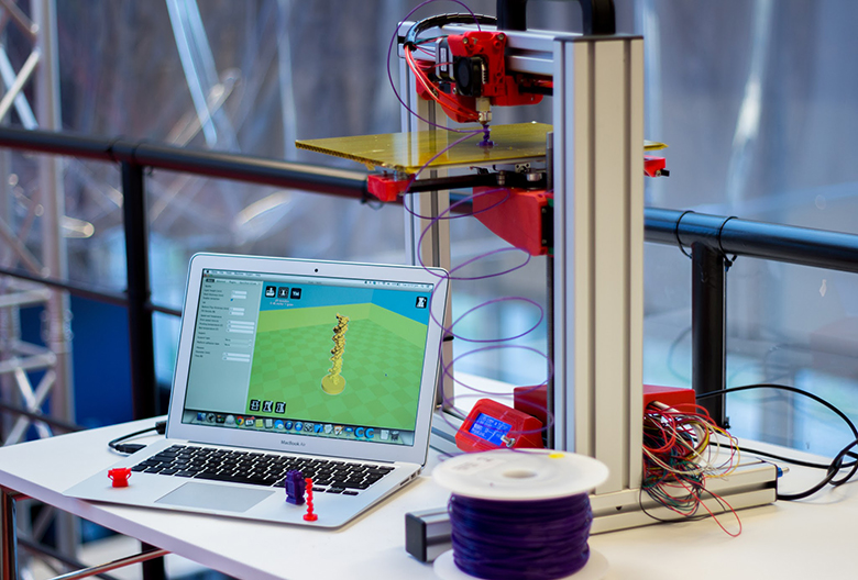
1. It’s For Prototyping – For Now
As mentioned above, 3D-printed PCBs aren’t for mass production just yet, but 3D printing is already changing the way PCBs are prototyped for electronic product designs today. Engineers can use 3D-printed breadboards to test out their designs that need to simulate microcontrollers. With 3D printing, you also don’t have to go through the hassle of etching a PCB yourself when creating a prototype.
2. How Do PCBs Work?
Most 3D printers designed for PCBs, like the Voxel 8, can print both conductive and non-conductive materials and can also print out different-size traces to match the needs of the model or size of the electronic product design. Other printers conveniently categorized as 3D printers for PCBs employ a combination of CNC machining and 3D printing to add and trace out the PCB model.
3. You Still Need Precision Software
Another issue with prototyping in the past has been testing. PCB prototyping often only requires one of a few boards to be tested. However, many PCB fabricators require a minimum quantity that far exceeds what is needed.
3D printing PCBs for electronic product designs greatly diminishes the back and forth of testing, as even complex prototype boards can be printed in under 20 minutes. That being said, making a PCB with a dedicated 3D printer still requires design expertise and precision software.
This is especially crucial if you’re fabricating more advanced PCBs with 3D printers that require a multi-layer stack-up manager. With the advent of 3D PCBs, many software tools today have a unified design environment to mitigate the need to use separate programs for divergent functions.
4. There are Currently Only 2 Methods Used
Not accounting for the 3D PCB printers that use CNC machining methods, the boards are printed using two methods:
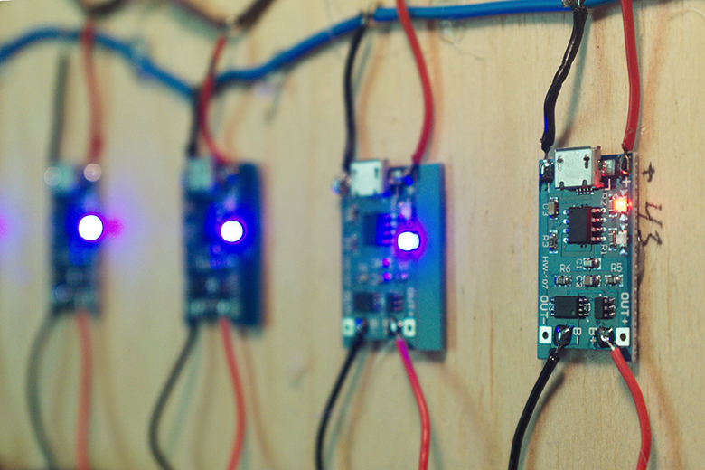
Using Conductive Filament. This method uses the 3D printer to lay down a conductive filament to create a pattern of lines similar to that on a regular PCB. With this method, you can create multiple layers of circuitry and incorporate other form factors on your substrate material.
Creating Hollow Traces. As the name suggests, this method prints hollow traces that can be filled with a conductive substance later on – either with electric paint or conductive epoxy.
The method you use generally boils down to your expertise and budget, as the first option is more complex but costs less than the second.
5. It Might be the Future of Electronic Product Design
Given the huge advantages of low cost and fast turnaround times in prototyping, 3D PCBs have the potential to catalyze innovation in electronic product design. In fact, studies are being done to maximize the technology of printing PCBs in wearables like fabrics and cloth. Another direction this is going is the integration of printing electronics and PCBs in one 3D printer like the NexD1 printer. While the project was discontinued, it’s a step towards adopting 3D-printed circuit boards in mass production.
As these five points show, 3D-printed circuit boards are rapidly becoming the norm. In the near future, expect 3D printing to be the only way to manufacture them.
If you have a great invention idea and you’d like to learn more about this process, get in touch with MAKO today, and we can set you up on a call with our product strategist!
About: MAKO Design + Invent is the original firm providing world-class consumer product development services tailored to startups, small manufacturers, and inventors. Simply put, we are the leading one-stop-shop for developing your physical product from idea to store shelves, all in a high-quality, cost-effective, and timely manner. We operate as one powerhouse 30-person product design team spread across 4 offices to serve you (Austin, Miami, San Francisco, & Toronto). We have full-stack in-house industrial design, mechanical engineering, electrical engineering, patent referral, prototyping, and manufacturing services. To assist our startup and inventor clients, in addition to above, we help with business strategy, product strategy, marketing, and sales/distribution for all consumer product categories. Also, our founder Kevin Mako hosts The Product Startup Podcast, the industry's leading hardware podcast. Check it out for tips, interviews, and best practices for hardware startups, inventors, and product developers. Click HERE to learn more about MAKO Design + Invent!