PCB Design and Its Role in Product Design:
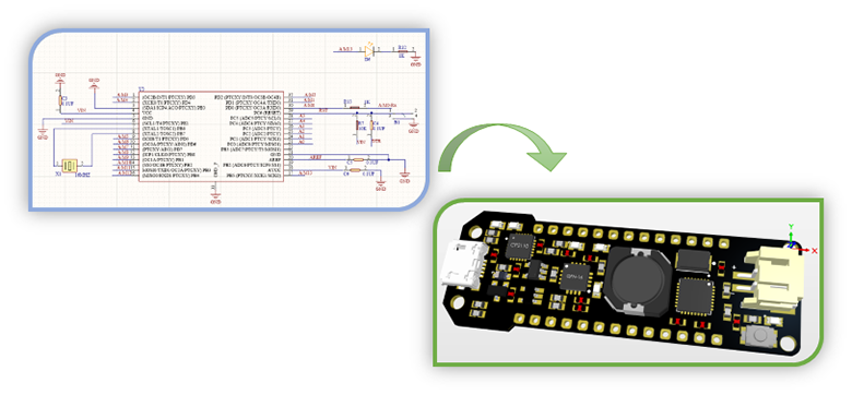
As an electrical design firm, we consider Printed Circuit Boards, or ‘PCBs,’ to be the brains inside most of the electronic products on the market today. From the basic automatic door opener to your multi-functional smartwatch, from the diagnostic ECG machine to high-speed supercomputers – each of these devices is driven by the PCBs. A PCB is an electrical circuit which consists of alternating layers of conducting copper and non-conducting insulating layers. The electrical components are connected through the copper layers and are mechanically supported by the insulating layers. The signals and power travel over traces and pads to different points on the PCB. The PCBs can range from a single-layer design to a multi-layer design with a rigid, flex, or flex-rigid implementation depending upon the density of components, complexity, space, and application constraints.
PCB Design is one of the most important steps for an electrical design firm during the making of an electronic product. How well the circuit is laid out on the PCB determines the overall performance of the device or product. A good PCB design must strike a balance between the functionality, cost-effectiveness, reliability, and design time while still satisfying the mechanical and manufacturing constraints. The ultimate goal of an optimal PCB design is to ensure that the basic schematic design is successfully translated to a layout that can be fabricated in an electronic circuit manufacturing environment and makes it possible to deliver more competitive products in less time.
Knowing Your Constraints:
Understanding the constraints early in the process makes the PCB design less prone to errors, saves costs, and design time. At an electrical design firm like Mako Design, we focus on understanding the final product in-depth, its desired features and functionality, target users, and how the PCB would be housed in the end-product. The significant constraints that must be considered are:
- Manufacturer constraints are one of the deciding factors for the final PCB design. Each fabrication firm has its own specifications, such as minimum trace width, board thickness, spacing, and a maximum number of layers. So, we have to choose a PCB manufacturer that can meet the design requirements, and hence collaborating with the PCB fabrication firm from the early design phase is a very significant step and has a tremendous effect on PCBs cost, yield, supply chain, and manufacturability.
- Most PCB manufacturers offer FR-4 as a default choice for substrate and 1oz (35 µm), 2 oz (70 µm), and 0.5 oz (18 µm) copper thickness are common options. The choice of materials impacts the board’s strength, moisture absorption, flame resistance, and durability. When designing high-speed designs or RF boards, the dielectricity and thickness of the material may require specialized manufacturing processes.
- If a PCB has a radio on it (such as Wi-Fi, Bluetooth), we may need to specify impedance control. For a consumer product, RoHS compliance is an important parameter which must be communicated to the fabrication firm. The cost of manufacturing scales with the PCB surface area and irregularly shaped PCB board designs are more expensive to fabricate.
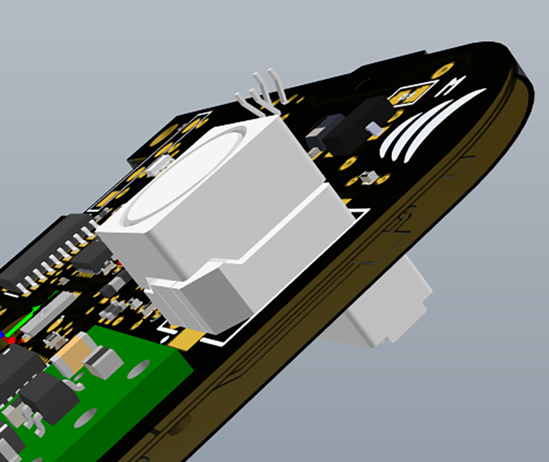
- PCB design for a product generally takes place in sync with the mechanical design- it’s essentially an intersection of mechanical and electrical design. The mechanical dimensions of the product determine the board outline and size. If the product’s package size is small and functionality is complex, it may require the electrical designer to shift to a multilayer board with surface mount components from a simple two-layer design. Other mechanical constraints can be height restrictions, mounting holes, and the number of boards in the product.
- The product’s ambient temperature range and operating environment are crucial parameters for component selection and PCB design.
Finding the Best-Fit Components and Their Placement:
- The component research and selection are the most fundamental to a successful PCB design. The datasheets provide detailed information such as operating points, switching characteristics, design considerations for components and can help the designer evaluate components to investigate how each works and how it can fit in the overall design. The package size, the electrical and mechanical footprints, and land patterns give a sense of component positioning and spacing on the PCB.
- During PCB design, a component exists as a virtual entity, but the product ultimately depends on its actual physical existence. If a component in the design database is no longer available or if a critical component reaches the end of life after entering high-volume production, it can result in severe problems such as product redesign and delayed production. So, optimizing component selection in PCB design is essential for product development. Checking components quantities from reliable suppliers, researching comparable replacements, having access to up-to-date component lifecycle data, and maintaining the Bill of Material (BOM) will help reduce the possibilities of delay and redesign.
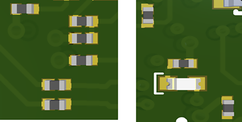
- The component placement in the PCB layout is both an art and a science, requiring a strategic consideration about the prime real estate available on your board. How the components are placed decides how easy or difficult the routing will be? The optimal placement maximizes the signal integrity and circuit performance while also adhering to spacing guidelines for thermal, electrical noise, mechanical, and manufacturing requirements. It enables the designers to plan for proper power distribution as well as critical signal routing on the PCB.
- Components must be segregated according to their functions- power, analog, and digital components should be grouped separately to minimize intersecting connection paths. Similar components should be oriented in the same direction to ensure effective routing and efficient soldering during assembly. The connectors, switches, and mechanical components such as nuts, bolts should be placed at fixed locations. It is always cost-effective to minimize the area of the PCB unless some components have specific rules for adjacent components and trace clearance
The best electrical design firms understand that a good component placement lays a solid foundation for a great PCB design and is probably one of the most challenging steps of the PCB design process. Once the placement is finished, it’s time to start routing!
Routing Guidelines:
There is no specific “formula” for good routing but here are some guidelines which can be utilized to achieve a reliable PCB design.
- The traces between components should be as short and direct as possible. If the component placement forces horizontal trace routing on one side of the board, the traces on the opposite side should be routed vertically. The PCB trace widths must be determined using calculations based on IPC-2152 to ensure proper current flow.
- The power and ground planes should be symmetrical, centered, and placed on the interior area of the board. Proper ground separation is important to ensure that digital signals do not interfere with the analog signals. Single point connections are usually recommended to keep analog and digital ground apart. Also, the power ground and control ground should be kept separate for each power supply stage. If they have to be tied together in the PCBs, make sure it’s toward the end of your supply path.
- Recommended practices for managing thermal issues include keeping critical components away from the heat sources, distributing the heat-generating components across the board, and adding thermal reliefs. Power management components should utilize ground planes or power planes for heat flow.
- Other best practices include using common rails for each supply, making sure you have reliable, extensive traces, and avoiding creating daisy chains to connect components. Special attention should be paid to sensitive signals which should be shielded from noise sources and be impedance controlled. For high current paths, placing multiple vias at layer transitions can reduce resistive and inductive losses, increase reliability, and improve thermal conductivity.
During the placement and routing steps, the Design Rule Check (DRC) is crucial as a practice within our electrical design firm as it helps the designer stick to the defined rules and constraints and identifies potential problems in the design. The DRC rules are programmed for each individual design and should be well researched and set to ensure a robust design. The final DRC check must be done to verify the correctness of the design.

Best Practices: 24-bit Parallel RGB Display Applications
Looking specifically at the products in which the PCB should include a 24-bit parallel RGB interface display, a special set of practices is recommended. The PCB layout requirements will primarily depend on the pixel clock and therefore on the required display resolution. The maximum length restrictions are defined due to electromagnetic radiation problems associated with the parallel interface.
The components datasheet is a good reference point for designing footprint and routing constraints. As the display is driven using parallel signals, these signals must feed the circuitry at the same time to avoid flickering. The signal traces should match in length with each other in order to have the same traveling time. The clock signal line should have a longer trace to guarantee that all the other signals are stable at the appropriate value when the clock triggers the frame. To achieve a certain trace length, serpentine traces are often needed. A minimum distance of four times the trace width between adjacent copper in a single trace must be used. If bends are needed, using 135° bends instead of 90° is recommended.
The PCB design practices mentioned here are just a few of the many that are required for an optimal design and are some that our electrical design firm practices frequently, as they serve as a basic guideline for many products. The best strategies and practices for any electronic product will largely depend on its requirements, complexity constituent components, and application. In very complicated PCB boards for specialized applications, many of the common PCB best practices may no longer apply, and one may need to follow PCB design guidelines that are suited to the specific product. Remember, every product design is unique and so is its PCB design!
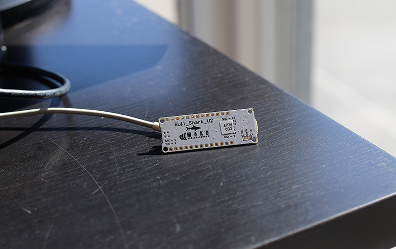
A look at one of our in-house, custom made PCB’s! The Bullshark V2
If you have a great new invention and you’d like to learn more about this process, get in touch with MAKO here and visit our website to find out more. Feel free to give us a call at 1-888-MAKO and we can set you up on a call with our product analyst!
About: MAKO Design + Invent is the original firm providing world-class consumer product development services tailored to startups, small manufacturers, and inventors. Simply put, we are the leading one-stop-shop for developing your physical product from idea to store shelves, all in a high-quality, cost-effective, and timely manner. We operate as one powerhouse 30-person product design team spread across 4 offices to serve you (Austin, Miami, San Francisco, & Toronto). We have full-stack in-house industrial design, mechanical engineering, electrical engineering, patent referral, prototyping, and manufacturing services. To assist our startup and inventor clients, in addition to above, we help with business strategy, product strategy, marketing, and sales/distribution for all consumer product categories. Also, our founder Kevin Mako hosts The Product Startup Podcast, the industry's leading hardware podcast. Check it out for tips, interviews, and best practices for hardware startups, inventors, and product developers. Click HERE to learn more about MAKO Design + Invent!
